Cost-Optimized Portfolio Overview
Cost-Optimized
The balance between feature set and affordability
Power Efficient
The balance between performance and power
Small Form Factor
The balance between physical size and logic resources
AMD ULTRASCALE+ COST-OPTIMIZED Devices
I/O, Power, Security-Optimized
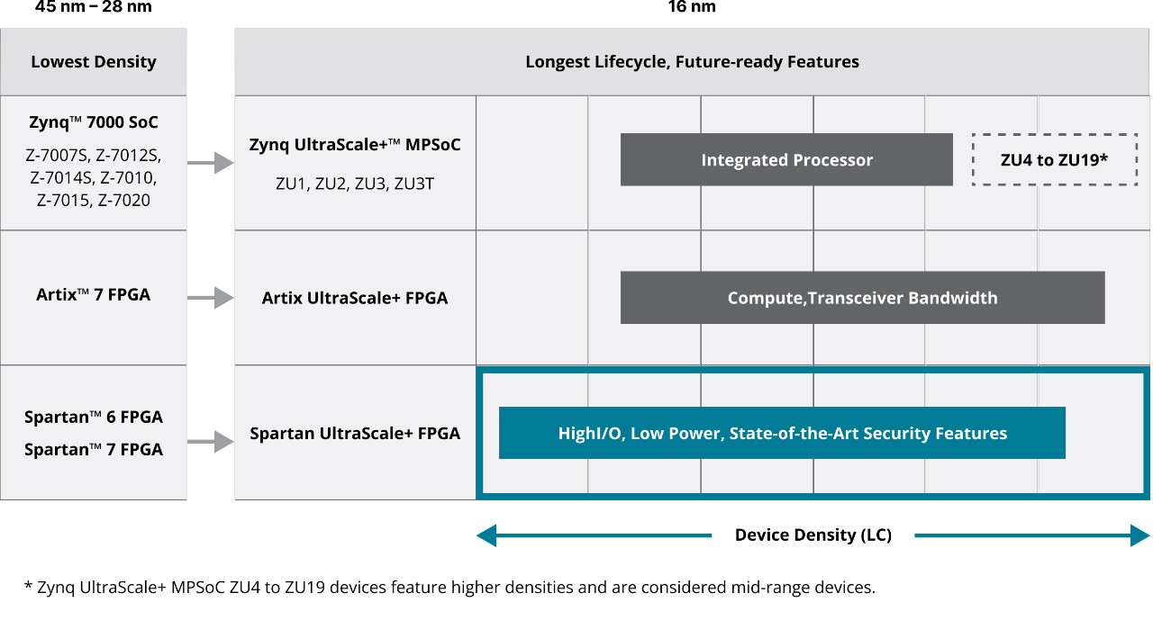
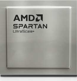
The AMD Spartan™ UltraScale+™ FPGA family is optimized for cost-sensitive applications requiring high I/O count, low- power, and state-of-the-art security features. With densities ranging from 11 kLC to 218 kLC and up to 572 I/Os, Spartan UltraScale+ FPGAs excel in a wide range of use cases, from I/O expansion and board management to sensor processing and control.
Transceiver and Signal Processing Optimized
The Artix™ UltraScale+™ FPGA offers high data throughput and DSP compute, providing up to 192 Gb of aggregate bandwidth. Key applications include embedded and video processing, wireless communications, advanced driver assistance systems (ADAS), and industrial IoT.
Embedded Processing Optimized
The Zynq™ UltraScale+™ MPSoC integrates the Arm® processor subsystem and UltraScale™ programmable logic architecture in a single device. Key applications include high-speed networking, high-performance computing, 5G wireless, automotive, avionics, and industrial control systems.
AMD 7 SERIES COST-OPTIMIZED Devices
Low Density and Smallest Packaging
The AMD Spartan™ 7 FPGA family offers an outstanding choice for low density and small form factor. With devices as small as 6K logic cells, engineers can do a lot with a little. Spartan 7 FPGAs pack 100 I/Os in a miniscule 0.5 mm pitch, 8x8 mm footprint as well as 0.8 mm and 1.0 mm pitch options. The devices are ideal for any-to-any connectivity, protocol conversion, bridging, sensor fusion, and embedded vision applications
Low Density with Transceivers and DSP
The AMD Artix™ 7 FPGA family provides up to sixteen 6.6 Gb/s transceivers, enabling efficient and robust data communication and DDR3 support for faster data bandwidth. Simultaneously, the DSP capabilities facilitate signal processing with high throughput. The family offers a great value for modest signal processing applications, such as software-defined radio and low-end wireless backhaul.
Low Density with Hardened Processors
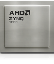
The AMD Zynq™ 7000 SoC family offers the smallest possible devices with hardened processors, embedded memory controllers, and 7 series programmable logic. The family offers devices as small as a single-core Arm® Cortex®-A9 processor running up to 766 MHz with 23K logic cells or a dual-core Arm Cortex-A9 processor running up to 866 MHz with 28K logic cells. Zynq 7000 SoCs are ideal for system management and flexible computing applications.
Unlocking Innovation with Cost-Optimized FPGAs and Adaptive SoCs
Innovations like machine vision and AI at the edge require new architectures that are flexible, energy efficient, and low cost. This eBook explores the differences between FPGAs, adaptive SoCs, ASICs, and other standard processors to help you decide which approach is best for your application. Learn how you can elevate your next design to meet the increasing complexity of today’s innovations without compromising on performance or efficiency.
DESIGN CONFIDENTLY
AMD takes our commitment to long lifecycles very seriously. We are pleased to announce that support is formally being extended for all 7 series devices through at least 2035. This includes all speed and temperature grades for Spartan™ 7, Artix™ 7, Kintex™ 7, and Virtex™ 7 FPGAs, as well as Zynq™ 7000 SoCs.
FIND THE RIGHT PRODUCT FAMILY
Solving diverse industry-specific problems with performance and flexibility
FPGA Cost-Optimized Devices
| Spartan™ 6 FPGA | Spartan 7 FPGA | Artix™ 7 FPGA | Artix UltraScale+™ FPGA | Spartan UltraScale+ FPGA | |
| Logic Cells / System Logic Cells (K) | 147 | 102 | 215 | 308 | 218 |
| Total RAM (Mb)1 | 6.2 | 5.4 | 16.0 | 15.2 | 26.79 |
| DSP Slices | 180 | 160 | 740 | 1200 | 384 |
| Transceiver Count @ Speed (Gb/s) | 8 @ 3.2 | - | 16 @ 6.6 | 12 @ 16.375 | 8 @ 16.375 |
| DDR Interface @ Speed (Mb/s) | DDR3 @ 800 (Hard MC) |
DDR3 @ 800 (Soft MC) |
DDR3 @ 1,066 (Soft MC) |
DDR4 @ 2,400 (Soft MC) |
LPDDR4x/5 @ 4,266 (Hard MC) and DDR4 @ 2,400 (Soft MC) |
| PCI Express® Interface | Gen1 x1 | - | Gen2 x4 | Gen4 x4 | Gen4 x8 |
| I/O Pins | 576 | 400 | 500 | 304 | 572 |
| Processing System | |||||
| Application Processor Unit | MicroBlaze™ | MicroBlaze V | MicroBlaze V | MicroBlaze V | MicroBlaze V |
| Real-Time Processor Unit | MicroBlaze | MicroBlaze V | MicroBlaze V | MicroBlaze V | MicroBlaze V |
| Graphics Processor Unit | 3rd Party IP | 3rd Party IP | 3rd Party IP | 3rd Party IP | 3rd Party IP |
| Memory Interfaces | DDR3 @ 800 (Hard MC) |
DDR3 @ 800 (Soft MC) |
DDR3 @ 1,066 (Soft MC) |
DDR4 @ 2,400 (Soft MC) |
LPDDR4x/5 @ 4,266 (Hard MC) and DDR4 @ 2,400 (Soft MC) |
SoC Cost-Optimized Devices
| Zynq™ 7000 SoC Z-7007S, Z-7012S, Z-7014S, Z-7010, Z-7015, Z-70202 |
Zynq UltraScale+™ MPSoC ZU1, ZU2, ZU3, ZU3T2 |
|
| Logic Cells / System Logic Cells (K) | 85 | 157 |
| Total RAM (Mb)* | 5.9 | 21.2 |
| DSP Slices | 220 | 576 |
| Transceiver Count @ Speed (Gb/s) | 4 @ 6.25 | 4 @ 6.0 and 8 @ 12.5 |
| DDR Interface @ Speed (Mb/s) | DDR3 @ 1,066 (Hard MC) |
DDR4 @ 2,666 (Hard MC) |
| PCI Express® Interface | Gen2 x4 | Gen3 x8 |
| I/O Pins | 328 | 466 |
| Processing System | ||
| Application Processor Unit | Single / Dual-core Arm® Cortex®-A9 | Dual / Quad-core Arm Cortex-A53 |
| Real-Time Processor Unit | MicroBlaze and MicroBlaze V | Dual-core Arm Cortex-R5F |
| Graphics Processor Unit | 3rd Party IP | Mali™-400MP2 |
| Memory Interfaces | DDR3, DDR3L, DDR2, LPDDR2, 2x Quad-SPI, NAND, NOR | x16: DDR4 w/o ECC; x32/x64: DDR4, LPDDR4, DDR3, DDR3L, LPDDR3 w/ ECC, 2x Quad-SPI, NAND |
- Total RAM = Maximum Distributed RAM + Total Block RAM + UltraRAM
- Larger devices up to Z-7100 and ZU19 also available
Not sure which family is right for your design? Check out our full Product Selection Guide
Featured Resources
JUMP-START YOUR EVALUATION
Get up and running quickly with development kits.


