AI Inference Acceleration
- Lowest latency AI inference
- Accelerate your whole application
- Match the speed of AI innovation

Lowest Latency AI Inference

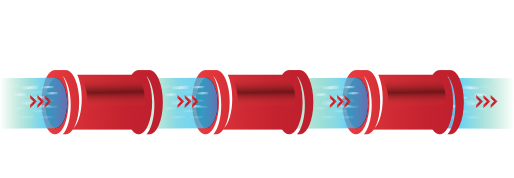
High Throughput OR Low Latency
Achieves throughput using high-batch size. Must wait for all inputs to be ready before processing, resulting in high latency.

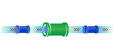
High Throughput AND Low Latency
Achieves throughput using low-batch size. Processes each input as soon as it’s ready, resulting in low latency.
Accelerate Your Whole Application

Optimized hardware acceleration of both AI inference and other performance-critical functions by tightly coupling custom accelerators into a dynamic architecture silicon device.
This delivers end-to-end application performance that is significantly greater than a fixed-architecture AI accelerator like a GPU; because with a GPU, the other performance-critical functions of the application must still run in software, without the performance or efficiency of custom hardware acceleration.
Match the Speed of AI Innovation
AI Models Are Rapidly Evolving

Adaptable silicon allows Domain-Specific Architectures (DSAs) to be updated,
optimizing the latest AI models without needing new silicon

Fixed silicon devices are not optimized for the latest models due to long development cycles

Vitis AI in the Data Center
AMD delivers the highest throughput at the lowest latency. In standard benchmark tests on GoogleNet V1, the AMD Alveo U250 platform delivers more than 4x the throughput of the fastest existing GPU for real-time inference. Learn more in the whitepaper: Accelerating DNNs with AMD Alveo Accelerator Cards

Vitis AI at the Edge
AI Inference performance leadership with Vitis AI Optimizer technology.
- 5X to 50X network performance optimization
- Increase FPS and reduces power
Optimization/Acceleration Compiler Tools
- Supports networks from Tensorflow and Caffe
- Compiles networks to optimized AMD Vitis runtime
