AMD Kintex 7 FPGA Connectivity Kit
by: AMD
The Kintex™ 7 FPGA Connectivity Kit is a 20Gb/s platform for high-bandwidth and high-performance applications containing all the necessary hardware, tools and IP to power quickly through your evaluation and development of connectivity systems.
Overview
Product Description
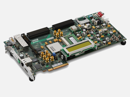
The Kintex™ 7 FPGA Connectivity Kit is a 20Gb/s platform for high-bandwidth and high-performance applications containing all the necessary hardware, tools and IP to power quickly through your evaluation and development of connectivity systems. This includes a 20Gb/s targeted reference design featuring PCI Express®, a DMA IP core from Northwest Logic, 10GBase-R, AXI, and a Virtual FIFO memory controller interfacing to an external DDR3 memory. To control and monitor this design, the board includes a connectivity GUI built on Fedora Live OS which includes all the software drivers. Additionally, this board contains the relevant SFP+ FMC daughter card, cable and transceiver modules needed to utilize this design.
Key Features & Benefits
- Optimized for quickly prototyping high performance serial transceiver applications using Kintex 7 FPGAs
- Hardware, design tools, IP, and pre-verified reference designs
- Demonstrates an Featuring 10GBase-R interfacing to external DDR3 memory
- Advanced memory interface with 1GB DDR3 SODIM Memory
- Enabling serial connectivity with PCIe Gen2x4, SFP+ and SMA Pairs, UART, IIC
- Supports embedded processing with MicroBlaze, soft 32bit RISC
- Develop networking applications with 10-100-1000 Mbps Ethernet (GMII, RGMII and SGMII)
- Implement Video display applications with HDMI out
- Expand I/O with the FPGA Mezzanine Card (FMC) interface
Featured AMD Devices
Featuring the ROHS compliant KC705 kit including the XC7K325T-2FFG900C FPGA
| Logic Cells | 326,080 |
|---|---|
| DSP Slices | 840 |
| Memory | 16,020 |
| GTY Transceivers | 16 |
| I/0 Pins | 500 |

Product Information
Board Features
Featuring the Kintex 7 Connectivity Board

Configuration
- Onboard JTAG configuration circuitry to enable configuration over USB
- 128MB (1024Mb) Linear BPI Flash for PCIe® Configuration
- JTAG header provided for use with AMD download cables such as the Platform Cable USB II
- 16MB (128Mb) Quad SPI Flash
Memory
- 1GB DDR3 SODIMM 800MHz / 1600Mbps
- 128MB (1024Mb) Linear BPI Flash for PCIe Configuration
- 16MB (128Mb) Quad SPI Flash
- 8Kb IIC EEPROM
- SD Card Slot
Communication & Networking
- GigE Ethernet GMII, RGMII and SGMII
- SFP / SFP+ cage
- GTX port (TX, RX) with four SMA connectors
- UART To USB Bridge
- PCI Express x8 edge connector
Display
- HDMI Video output
- External Phy/codec device driving an HDMI Connector
- 2x16 LCD display
- 8x LEDs
Clocking
- Fixed Oscillator with differential 200MHz output used as the “system” clock for the FPGA
- Programmable Oscillator with 156.250 MHz as the default output - default frequency targeted for Ethernet applications but oscillator is programmable for many end uses
- Differential SMA clock input
- Differential SMA GTX reference clock input
- Jitter attenuated clock used to support CPRI/OBSAI applications that perform clock recovery from a user-supplied SFP/SFP+ module
Expansion Connectors
- FMC-HPC (Partial Population) connector (4 GTX Transceiver, 116 single-ended or 58 differential (34 LA & 24 HA) user defined signals)
- FMC-LPC connector (1 GTX Transceiver, 68 single-ended or 34 differential user defined signals)
- Vadj can support 1.8V, 2.5V, or 3.3V
- IIC
Power
- 12V wall adapter or ATX
- Voltage and Current measurement capability of 2.5V, 1.5V, and 1.2V, 1.0V supplies (IIC path to FPGA)
Analog
- XADC header
Control & I/O
- 5X Push Buttons
- 4X DIP Switches
- Diff Pair I/O (1 SMA pair)
- AMS FAN Header (2 I/O)
- 7 I/O pins available through LCD header
What's Inside
Kintex 7 FPGA Connectivity Kit
Featuring the XC7K325T-2FFG900C FPGA

Full seat Vivado™ Design Suite: Design Edition
Node locked & Device-locked to the Kintex 7 XC7K325T FPGA, with 1 year of updates

S14 FMC Daughter Card
Featuring ganged SFP cages supporting up to 4x SFP+ modules from Faster Technology

Ethernet Cable

USB Micro Cable

USB Mini Cable

Power Adapter and Power Cord

Two 10Gb Ethernet transceiver modules and a single fiber optic patch cable


Resources
Design Tools
| Name | Description | License Type |
|---|---|---|
| Vivado Design Suite Design Edition | The AMD Vivado™ Design Suite is a revolutionary IP and System Centric design environment built from the ground up to accelerate the design for FPGAs and SoCs. | Node locked & Device-locked to the Kintex 7 XC7K325T FPGA, with 1 year of updates |
Intellectual Property
| Name | Description | License Type |
|---|---|---|
| PCI Express DMA Engine (Northwest Logic) | Northwest Logic’s PCI Express DMA Back-End Core | Hardware Time Out Evaluation license for the Northwest Logic DMA implemented with and limited to an AXI DMA Back-End interface >> See More |
| Memory Interface Generator (MIG) | MIG is a free software tool used to generate memory controllers and interfaces for AMD FPGAs | No-Charge IP |