
Verification and Debug
Overview
Verification and HW Debug is critical to ensure the functionality, performance, and reliability of the final FPGA implementation. Vivado’s verification features enable efficient validation of design functionality while its comprehensive debugging features empower engineers to efficiently locate and resolve issues within complex FPGA designs.
Features
Simulation Flow
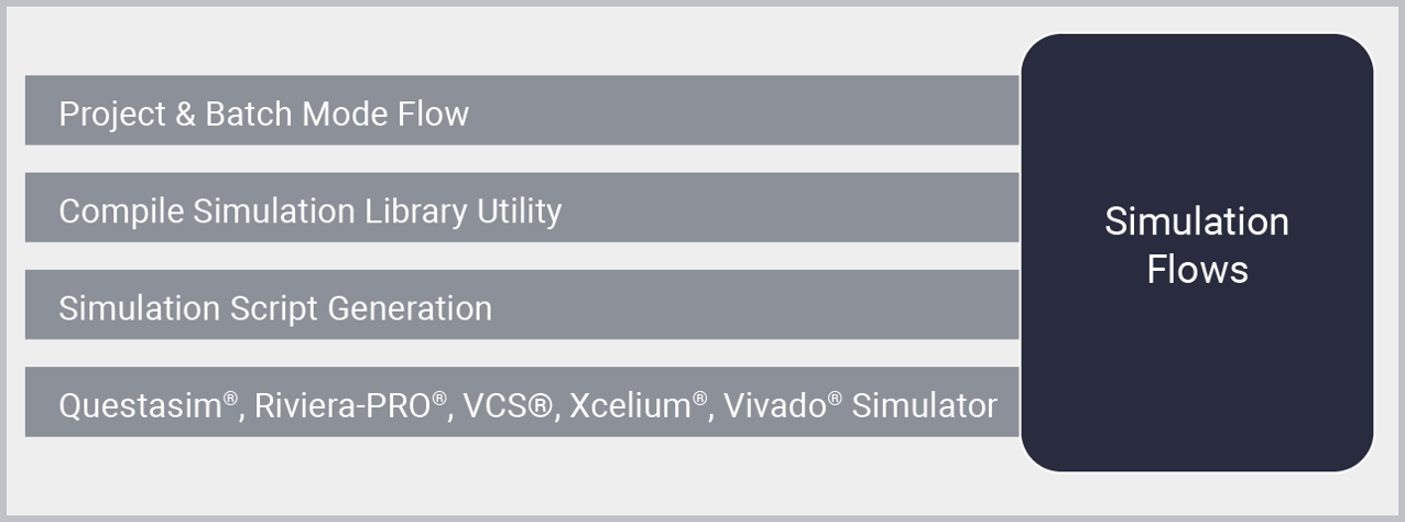
The Vivado™ Design Suite provides an array of design entry, timing analysis, hardware debug, and simulation capabilities all encompassed in a single state of the art integrated design environment (IDE). This flow enables both the integrated and enterprise verification needs for all supported simulators.
Vivado enables behavioral, post-synthesis and post-implementation (functional or timing) simulations for the fully integrated Vivado Simulator and 3rd party HDL simulators. Time spent on simulation early in the design cycle helps identify issues early and significantly reduces turnaround times compared to later stages of the flow.
To aid flexibility in user verification environments, Vivado provides support for both an integrated environment as well as provides scripts to use with external verification setups.
The Vivado IDE supports all major simulators in integrated mode for interactive simulation users and script mode for advanced verification engineers.
Aldec - Active-HDL® & Riviera-PRO®, Cadence Xcelium® Simulator, Siemens EDA – ModelSim® & Questasim®, Synopsys VCS® and AMD Vivado Simulator
Key Features
- Simulation flows provide the ability to compile simulation libraries for the supported simulators in the users’ environment to enable re-use of compiled libraries.
- Ability to simulate and verify design integrity at different stages of the design process such as behavioral, post -synthesis functional and timing simulation and Post-implementation functional and timing simulation.
- Unified simulation integration using consistent 3 step process (compile, elaborate, simulate) for all simulators
- Simulation script generation for enterprise 3rd party simulators to enable verification using users own environments.
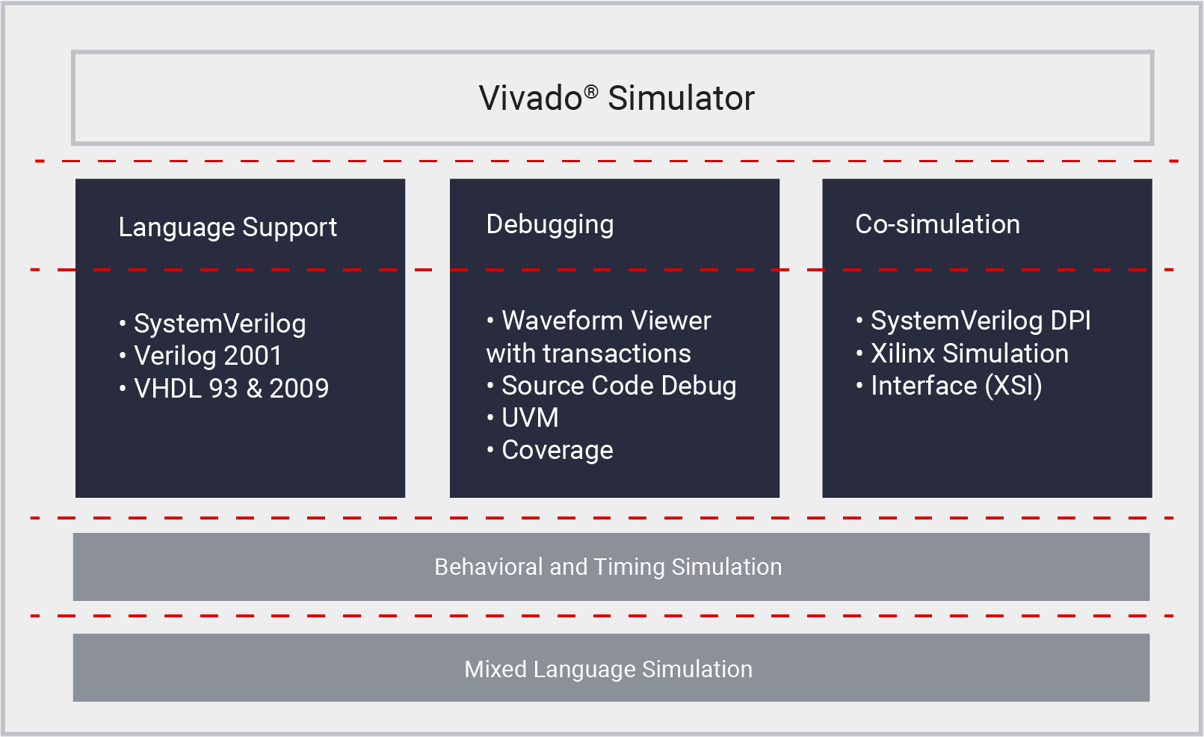
Vivado Simulator
Vivado™ Simulator is a feature-rich, mixed-language simulator that supports Verilog, SystemVerilog, and VHDL language. Vivado Simulator is included is part of Vivado and it is available at no additional cost. It does not have a design size, instances, or line limitation and it allows to run of unlimited instances of mixed-language simulation using a single Vivado license.
Vivado Simulator supports both Windows® and Linux operating systems with powerful debugging features that are aimed to address the verification needs of AMD customers.
Vivado Simulator is a hardware description language (HDL) event-driven simulator that supports behavioral and timing simulation for single language and mixed language designs.
Key Features
- SystemVerilog (Including constraint randomization and functional coverage)
- Verilog 2001
- VHDL 93 and VHDL 2008
- Advanced waveform viewer that supports digital/analog waveform & transaction view
- Comprehensive debugging tools such as breakpoints, subprogram debug and cross-probing
- Support for UVM 1.2 library
- Functional Coverage
- Support both GUI and script mode
- Direct programming interface (DPI)
- Xilinx simulation interface (XSI)


Programming and Debug
Vivado™ Debug offers a variety of solutions to help users debug their designs easily, quickly, and more effectively. These solutions consist of tools, IPs, and flows that enable a wide range of capabilities from logic to system level debug while the user design is running in hardware.
In addition, Vivado provides a unified design environment that enables you to perform different debug tasks within the same IDE in which interfaces look consistent and features communicate well with each other.
Highlights
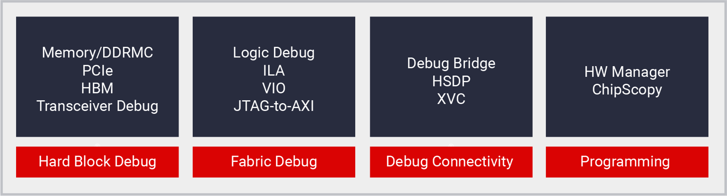
As part of Vivado IDE, Hardware Manager enables users to program the device and debug the design after bitstream generation. Using Hardware Manager, users connect and program hardware targets containing one or more FPGA devices and then interact with debug IPs in designs via Tcl or GUI interfaces including Logic Analyzer, Serial I/O Analyzer, and Memory Calibration Debug.
- Device programmer for FPGA, configuration memory devices, eFUSE AES key/registers
- Tcl scripting support for debug automation
- Remote debugging over network via hw_server & Xilinx Virtual Cable (XVC)
Vivado provides various debug IP and tool features that enable you to easily perform in-system logic debugging of your implemented design.
- ILA – used for triggering on events and capturing the data from internal signals
- System ILA - used for transaction-level debug of AXI interfaces
- VIO – used for monitoring and driving internal signals
- JTAG-to-AXI – used for direct interaction with AXI interfaces via Tcl
Vivado offers you a fast and easy method to debug and optimize FPGA transceivers. This solution includes a customizable debug IP (IBERT) and Vivado Serial I/O Analyzer tool. Used together, you can take bit-error ratio (BER) measurements on multiple channels, perform 1D/2D eye scans, and adjust transceiver parameters in real-time while your serial I/O channels interact with the rest of the system.
Designed for PMA evaluation and demonstration of transceivers, IBERT also includes data pattern generators and checkers as well as access to transceivers' DRP ports. Once IBERT is implemented within the FPGA, Vivado Serial I/O Analyzer interacts with the IP and allows you to create links (analogous to a channel on a board) and analyze the margin of the links by running scans and viewing the results graphically.
Memory Calibration Debug tool allows you to quickly debug calibration or data errors in memory interfaces (DDR4/3, RLDRAM3, QDRII+, and LPDDR3). You can always view and analyze core configuration, calibration status, and data margin of the memory interfaces at any time throughout the operation in hardware.
Xilinx Virtual Cable (XVC) solution is a TCP/IP-based protocol that acts like a JTAG cable and provides a way to access and debug your FPGA or SoC design without using a physical cable. XVC solution has both hardware and software components:
ChipScopy is a Python API that allows device programming, communication, and debug for Versal devices only. The high-level Python functions allow TCF server connection, device programming, read/write memory, trigger and capture ILA data & read/write VIO registers. It also allows running IBERT scans and sweeps, reading system monitor data, monitoring NOC performance , and reporting DDR Metrics.

Verification IP
Verification IP (VIP) portfolio by AMD provides users with the ability to verify and debug their designs in a simulation environment easily, quickly, and more effectively. Verification IP cores are purpose built verification models whose goal is to ensure correct interoperability and system behavior. Companies in the EDA industry develop VIP for standards based interfaces (AXI, PCIe, SAS, SATA, USB, HDMI, ENET, etc..). Advantages to using VIP include improved design quality and reduced schedule time due to re-usability.
AMD VIP cores are SystemVerilog based simulation models that provide full AXI protocol checking with ARM licensed assertions, support all major simulators, and are included in Vivado at no cost. AMD provides VIP for use in designs that use AXI component level (AXI-MM, AXI_Stream) and Processing System(Zynq™ 7000) designs.
Key Features
- AXI Traffic Generator for AXI4, AXI4-Stream, AXI4-Lite
- Full AXI & AXI Stream Protocol Checker support
- Functional simulation support for Zynq 7000 & Zynq US+ MPSoC based application
- Functional simulation support of Control, Interfaces, and Processing System (CIPS) IP
Resources

Documentation Portal
Robust online search and navigation of HTML-based technical content.

Design Hubs
Current technical content for specific design tasks, devices, and tools.

Training
Access our library of training materials across a variety of subjects.

Support Community
Expert Support, Design Advisories, Known Issues & Community.