Low Latency Transceiver Designs for Quantitative Finance
Abstract
Quantitative finance applications require the lowest latency transceiver implementations. In order to achieve this, several advanced transceiver features must be enabled simultaneously. These include RX and TX buffer bypass, as well as locking the transmitter timing to the receiver timing with FRACXO. This article describes how to do this as well as provide a tested reference design with latency measurement for a 10GbE transceiver on an Alveo™ U200 QSFP port. Xilinx® Vitis™ unified software platform is used to target a MicroBlaze to modify the Si570 transceiver reference clock frequency via I2C to support FRACXO requirements.
Introduction
Quantitative financial technology (Fintech) applications require ultra low latency information paths. A key differentiator in hardware platforms supporting Fintech applications is the latency from the receive port to the transmit port. In their simplest form, these systems are looking at information on a receive port, making a decision on that information, and inserting information on a transmit port. Most Fintech systems today employ 10G Ethernet for these ports. A key hardware element in the low latency path from receive to transmit is the transceiver itself. All else being equal this single element can provide the latency edge over other competitors. The most important elements of a transceiver that determine latency are data path width, data path frequency, and buffering. In addition, features that minimize the receive to transmit clock domain crossing latency are required. The Xilinx UltraScale family of transceivers can optimize for latency by controlling all of those.
Latency Platform Development
In order to develop a platform for evaluating latency on UltraScale transceivers, Vivado 2019.1 and the Vitis tool can be used quite easily on an Alveo U200 data center accelerator card. More information on the U200 can be found here: /content/xilinx/en/products/boards-and-kits/alveo/u200.html. Vivado is used to develop the block design (bd) employing a transceiver example design for data generation and reception and incorporate a microblaze processing element to control a board clock in order to optimize the receiver to transmit domain crossing. XAPP1276 (/content/xilinx/en/support/documentation/application_notes/xapp1276-vcxo.pdf), or FRACXO, is required to lock the receive clock to the transmit clock reducing the clock domain crossing latency to single fabric clock period.
The U200 has two QSFP+ ports with default GT reference clocks of 156.25 MHz. Although these ports support 100 GbE over four lanes, each lane of a QSFP+ port will also support a 10 GbE line rate of 10.3125G. Implementing FRACXO on a U200 for 10.3125G requires using the on board programmable Silabs Si570 clock oscillator since the fractional QPLL tuning range is from N to N+1. Therefore, you need to pick a nominal GT reference clock frequency that puts you in the center.
Solving for the Si570 clock: 10.3125G/(66+0.5) = 155.075188 MHz which will tune from 10.2349624GHz (div 66) to 10.39003759 GHz (div 67) which is far greater that the required +/-200 ppm for ethernet.
IBERT is used to verify complete operation. If FRACXO and buffer bypass combined do not provide a complete clocking solution capable of passing data through the QSFP0 port, errors will show up in IBERT.
Below is a simple block diagram for the reference design used to measure latency on the U200.
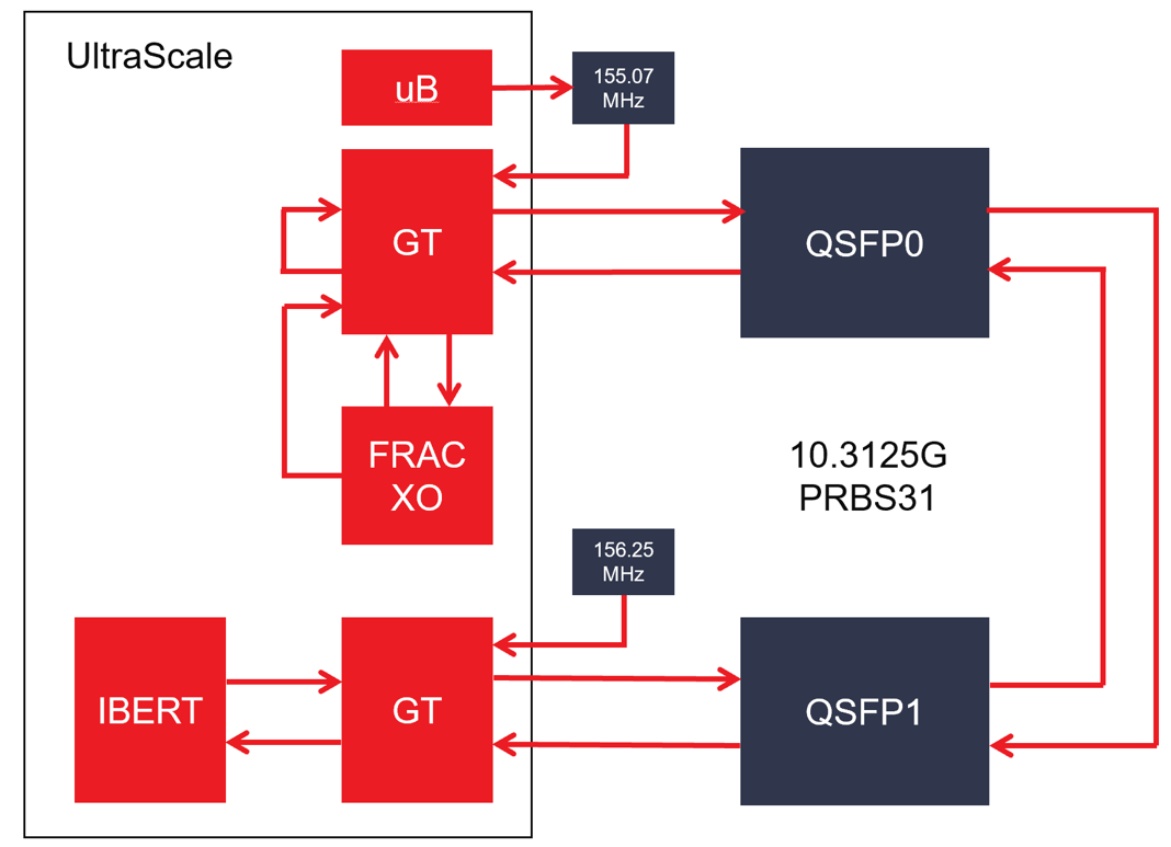
Producing the HW reference design
- Create FRACXO example design from IP default configuration @ 10.3125G.
- Create GT wizard example design @ 10.3125G/155.075187M with same configuration as FRACXO example design.
- RX and TX buffers bypassed and reset, buffer bypass, and clocking helper blocks in example design.
- Copy and paste FRACXO related items from FRACXO example design into GT wizard example design.
- Disable PRBS generator, wrap RX data to TX data, and make TXOUTCLK master of TXUSRCLKs/RXUSRCLKs.
- Set RXSYNC_SKIP_DA = 1'b1 in xdc to operate RX as a slave and skip delay alignment.
- Put FRACXO on QSFP0 Quad 231 - use Silabs programmable Si570 clock on refclk0.
- Add IBERT design on QSFP1 Quad 230 - use default 156.25MHz on refclk1.
- Add MicroBlaze processor subsystem with i2c peripheral to control Si530 refclk0.
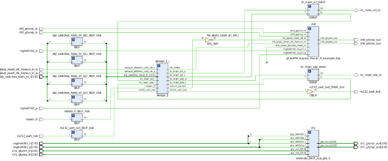

Producing the SW reference design
- After bitstream generation in the Vivado 2019.1 tcl console export dsa with write_dsa -fixed -include_bit u200.dsa
- Open the Vitis software platform and create new SDK Application project using the u200.dsa.
- Modify i2c si570 c code found in XAPP742 to adapt to the U200 to program to QSFP0 GT to 155.075187 MHz.
Latency Evaluation
Three modes of operation were evaluated for latency – 32-bit, 20-bit, and 16-bit data path widths. Calculated vs. measured was evaluated for total roundtrip (RX-to-TX). Please note that 32-bit and 20-bit data path designs are supported natively with production devices and speed files. 16-bit designs will produce pulse width timing violations but can still be used for evaluation purposes. Please contact Xilinx for additional support required for 16-bit data path designs at 10.3125G. The following answer record provides detailed latency information for the UltraScale+ GTY transceiver used on the Alveo U200. /content/xilinx/en/support/answers/69011.html
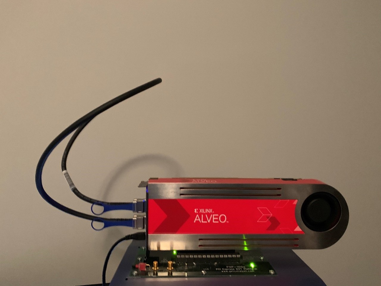
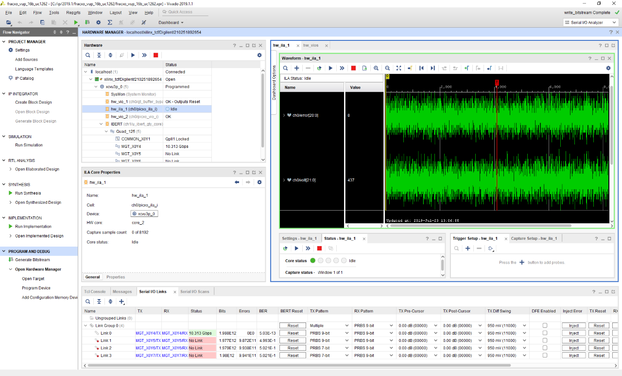
First, the U200 was checked for good signal integrity from QSFP0 to QSFP1 via a copper 1m QSFP cable. IBERT results along with a picture of the test setup are shown below. Note that the default configuration of the U200 results in QSFP0/1 refclk1 being set to 161.1328 MHz. A simple run-time setting on IBERT (if generated for using 156.25 MHz) to adjust the QPLL divide factor from 66 to 64 was necessary to get the desired 10.3125G line rate.

Using the Alveo test setup above the design was verified via JTAG. Vitas was used to program the SiLabs Si570 part to 155.075187 MHz. Note that the HW manager snapshot below shows a single channel of 10.3125G IBERT traffic looping from QSFP1 through the QSFPO error free retimed by FRACXO. The ILA capture shows the FRACXO status showing low error and voltage indicating lock. If FRACXO was not locked, and adequate timing margin did not exist in the fabric with the transceiver in buffer bypass, data would not be able to pass error free. This validates the complete design with all features for ultra low-latency.
The latency scope measurements were obtained on an internal evaluation board due to available SMA connections to make the measurement. While these same measurements could have been done on the Alveo u200, the QSFP breakout boards required were not available at the time of this write-up. Regardless, the latency measurements will be identical on any UltraScale Plus transceiver.
Latency Results: Measured versus Calculated
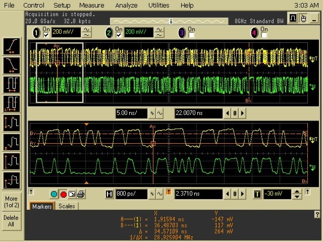
32-bit data width buffer bypass
Calculated latency:
- TX = 32+32+32+16+29 = 141 UI
- RX = 52.5+16+32+32 = 132.5 = 133 UI
- Total = 274 UI = (274)*1/10.3125G = 26.570 ns
Measured latency:
- Used a PRBS9 to measure RX-TX roundtrip latency since pattern is 511 UI (49.55ns) so it doesn't repeat during GT delay.
- Scope measurement (looking for 9 ones pattern) delay is 34.5ns.
- Calculate board and cable delay.
- Samtec 24in cable assembly HDR-155805-01-BEYE delay ~4.72ns/m. So cable delay is 39.3701in/m /(24in*2)/(4.72ns/m) = 5.75ns
- UC1262 Q124 TX = 2990 mils Q124 RX = 2730 mils ~ 160ps/in. So PCB delay is (2.99 + 2.73) * 0.160ns = 0.9152ns
- Total Board+cable delay (not accounting for scope and misc adapters - bullets, dc blocks, bnc to sma) = 6.6698ns
- Total TX+RX roundtrip delay measured = 34.5ns - 6.6698ns = 27.83ns
20-bit data width buffer bypass
Calculated latency:
- TX = 20+20+20+10+19 = 89 UI
- RX = 42.5+10+20+20 = 92.5 = 93 UI
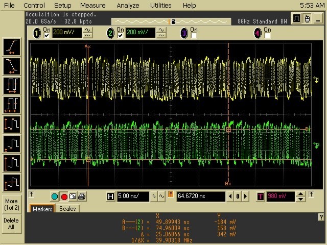
- Total = 182 UI = (182)*1/10.3125G = 17.65 ns
Measured latency:
- Scope measurement (looking for 9 ones pattern) delay is 25.1ns.
- Subtract out fixture delays as above.
- Total TX+RX roundtrip delay measured = 25.1ns - 6.6698ns = 18.43ns
16-bit data width buffer bypass
Calculated latency:
- TX = 16+16+16+8+19 = 75 UI
- RX = 36.5+8+16+16 = 76.5 = 77 UI
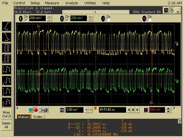
- Total = 152 UI = (152)*1/10.3125G = 14.739 ns
Measured latency:
- Scope measurement (looking for 9 ones pattern) delay is 21.50ns.
- Subtract out fixture delays as above.
- Total TX+RX roundtrip delay measured = 21.5ns - 6.6698ns = 14.83ns
Conclusion
UltraScale transceivers are capable of extremely low latency when using advanced features such and RX and TX buffer bypass, reduced data path width, higher operating frequency, and FRACXO to lock the RX to TX clock to avoid a clocking domain crossing FIFO. Vivado and Vitis technology can be easily used to produce both HW and SW designs for validation of transceiver latency on Alveo boards
Appendix A: Modifying GT data width and common clocking
In the default 32-bit data width generated GT example design, some constraints and RTL need to be manually modified for 16/20-bit data path widths and common clocking.
1) Modify user data width related variables inside *example_top.v
    wire [15:0] gtwiz_userdata_tx_int;
wire [15:0] hb0_gtwiz_userdata_tx_int;
assign gtwiz_userdata_tx_int[15:0] = hb0_gtwiz_userdata_tx_int;
wire [15:0] gtwiz_userdata_rx_int;
wire [15:0] hb0_gtwiz_userdata_rx_int;
assign hb0_gtwiz_userdata_rx_int = gtwiz_userdata_rx_int[15:0];
2) Modify *example_wrapper.v file.
    input wire gtwiz_userdata_tx_in[15:0]
output wire gtwiz_userdata_rx_out[15:0]
  // The source clock is RXOUTCLK from the master receiver channel
  // Make TXOUTCLK master of RXUSER clocks
  assign gtwiz_userclk_rx_srcclk_out = rxoutclk_int[P_RX_MASTER_CH_PACKED_IDX];
  //assign gtwiz_userclk_rx_srcclk_out = gtwiz_userclk_tx_srcclk_out;
  assign gtwiz_userclk_rx_usrclk_out = gtwiz_userclk_tx_usrclk_out;
  assign gtwiz_userclk_rx_usrclk2_out = gtwiz_userclk_tx_usrclk2_out;
  assign gtwiz_userclk_rx_active_out = gtwiz_userclk_tx_active_out;
  // Instantiate a single instance of the receiver user clocking network helper block
  gt_buffer_bypass_fracxo_0_example_gtwiz_userclk_rx gtwiz_userclk_rx_inst (
    .gtwiz_userclk_rx_srcclk_in   (gtwiz_userclk_rx_srcclk_out),
    .gtwiz_userclk_rx_reset_in    (gtwiz_userclk_rx_reset_in),
    .gtwiz_userclk_rx_usrclk_out  (),
    .gtwiz_userclk_rx_usrclk2_out (gtwiz_userclk_rx_usrclk2_fracxo_out),
    .gtwiz_userclk_rx_active_out  ()
  );
Make gtwiz_userclk_rx_usrclk2_fracxo_out a port and drive the ref_clk_i port of the FRACXO instance one level up in the *example_top.v module.
3) Additional blocks might need to be modified for a full simulation pass
    - *example_stimulus_raw.v
output wire [31:0] txdata_out
.NBITS       (16)
.DATA_IN  (16'b0),
- *_example_checking_raw.v
input  wire [15:0] rxdata_in,
wire [15:0] prbs_any_chk_error_int;
.NBITS       (16)
4) Unmanage the GT IP per UG896 Appendix D
5) Modify *gtwizard_ultrascale_0.v file.
    input wire [16:0] gtwiz_userdata_tx_in;
output wire [16:0] gtwiz_userdata_rx_out;
C_RX_INT_DATA_WIDTH = 16
C_RX_USER_DATA_WIDTH = 16
C_TX_INT_DATA_WIDTH = 16
C_TX_USER_DATA_WIDTH = 16
C_RX_OUTCLK_FREQUENCY = 644.53125
C_RX_USRCLK_FREQUENCY = 644.53125
C_RX_USRCLK2_FREQUENCY = 644.53125
C_TXPROGDIV_FREQ_VAL = 644.53125
C_TX_OUTCLK_FREQUENCY = 644.53125
C_TX_USRCLK_FREQUENCY = 644.53125
C_TX_USRCLK2_FREQUENCY = 644.53125
6) Modify *channel_wrapper.v file.
    .GTYE4_CHANNEL_TX_PROGDIV_CFG                 (8.0),
.GTYE4_CHANNEL_TX_DATA_WIDTH                  (16),
.GTYE4_CHANNEL_RX_DATA_WIDTH                  (16),
.GTYE4_CHANNEL_TX_INT_DATAWIDTH               (0),
.GTYE4_CHANNEL_RX_INT_DATAWIDTH               (0),
7) Modify the *fracxo_0_ooc.xdc file:
    create_clock -period 1.551 [get_ports txusrclk_in[0]]
create_clock -period 1.551 [get_ports txusrclk2_in[0]]
create_clock -period 1.551 [get_ports rxusrclk_in[0]]
create_clock -period 1.551 [get_ports rxusrclk2_in[0]]

About Howard Ireland
Howard Ireland has an M.S.E.E. from Johns Hopkins. He has a solid ASIC and FPGA design background in optical, cable, and satellite telecommunications systems as well as RF design background in radar systems. He holds eight patents. He currently works as a SERDES and RF Specialist for AMD.