- Applications
- Emulation and Prototyping
- ASIC Emulation in Action
ASIC Emulation in Action
Breakthrough performance and integration for ASIC and SoC emulation
Hardware emulation is the process of debugging and functional verification of the system in development. Comprehensive hardware functional verification is critical to reduce development cost and time-to-market. Emulation provides quick bring-up and quick turn-around time when processing design changes. Also, emulation provides high design accessibility and debug visibility so that ASIC designers can catch potential hardware failures before the tape out. As software complexity and cost are drastically increasing, early hardware verification is essential to lower risk and accelerate system development.
To maximize system performance and enable accelerated and predictable design cycles with emulators, AMD delivers the most comprehensive design methodology and design development platform. The Vivado™ Design Suite has delivered state-of-art development experience to emulation-class system designers. This is the 3rd generation AMD emulation-class tools, IP, and design flows.
For emulation platforms, AMD solutions :
- Enable large designs to eliminate the need for multi-chip partitioning in many instances
- Mitigate development risks for large ASIC and ASSP designs by providing fast place-and-route
- Reduce system-level power consumption
- Enable high utilization by ASIC-like clocking and routing architecture
- Deliver advanced debug and emulation acceleration
Featured Alliance Member
With the Virtex™ 7 2000T FPGA and the Virtex UltraScale™ VU440 FPGA, AMD has been the market leader for the highest capacity FPGAs. The 16nm Virtex UltraScale+™ family now includes the world’s largest FPGA, the Virtex UltraScale+ VU19P FPGA, achieving three consecutive generations of high-end leadership.
Virtex 7 2000T
Built with ASIC emulation in mind
- 2M logic cells, 6.8B transistors
- 36x 12.5Gb/s serial transceivers
- 46Mb of block RAM
- 1,200 I/Os
- 1st generation SSI technology
Virtex UltraScale VU440
Extending device density lead to 4X at 20nm
- 5.5M system logic cells, 20B transistors
- 48x 16.3Gb/s serial transceivers
- 89Mb of block RAM
- 1,456 I/Os
- 2nd generation SSI technology
Virtex UltraScale+ VU19P
Industry’s highest capacity FPGA
- 9M system logic cells, 35B transistors
- 80x 28Gb/s serial transceivers
- 94.5Mb of block RAM
- 2,072 I/Os
- 3rd generation SSI technology
Documentation
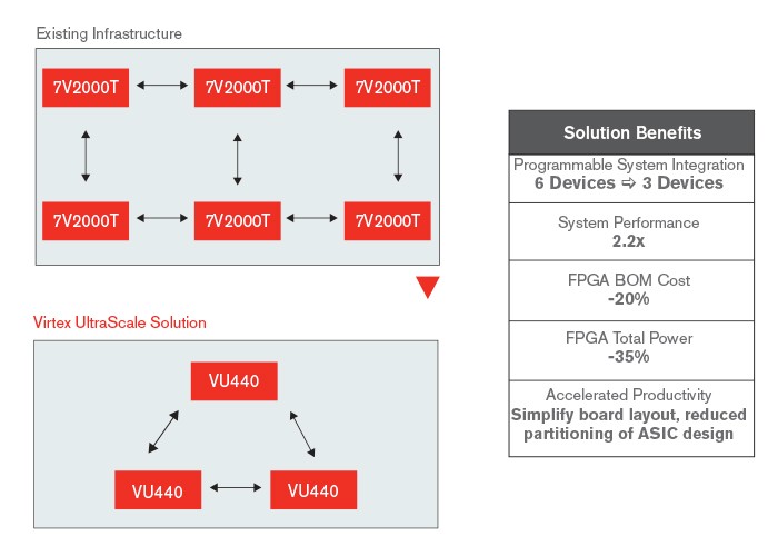
Breakthrough performance and integration for ASIC prototyping and emulation can be realized with AMD UltraScale™ architecture. Virtex™ UltraScale devices simplify design partitioning through high logic capacity, over 90% device utilization, ASIC-like clocking, enhanced routing, and high-speed transceivers for pin multiplexing. This breakthrough architecture coupled with Vivado™ Design Suite provides the ideal solution for tackling the demands of leading-edge ASIC and SoC platforms.
Solution Summary and Benefits
- Breakthrough device capacity reduces the number of partitions and simplifies board layout
- Enhanced routing and co-optimization with the Vivado Design Suite ensures over 90% device utilization
- ASIC-like clocking efficiently maps complex ASIC and SoC clock trees
- High-speed transceivers enable efficient pin multiplexing between FPGAs and support the I/O interfacing requirements for next generation systems
UltraScale Architecture Benefits
- Massive I/O Bandwidth
- > 1 Tbps chip to chip bandwidth available
- Low latency transceiver enables chip/chip interconnect
- Massive Data Flow & Routing
- Supports native wide ASIC busses with high performance
- Supports native wide ASIC busses with high performance
- ASIC-like Clocking
- Maximum flexibility for complex SoC prototyping
- Maximum flexibility for complex SoC prototyping
- System Peformance
- 15-30% performance improvement per device
- 3X improvement due to reduced partitioning
- Power Management
- Up to 35% System Power reduction
