AMD Virtex 7 FPGA VC709 Connectivity Kit
by: AMD
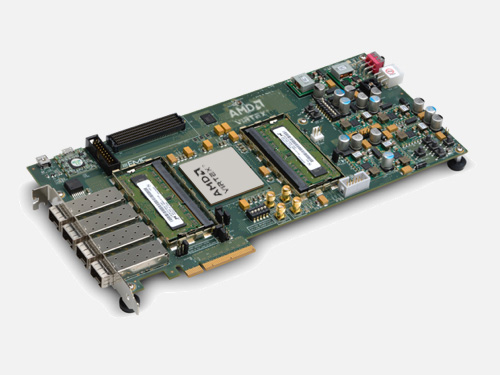
The Virtex™ 7 FPGA VC709 Connectivity Kit is a 40Gb/s platform for high-bandwidth and high-performance applications containing all the necessary hardware, tools and IP to power quickly through your evaluation and development of connectivity systems.
Overview
Product Description
The Virtex™ 7 FPGA VC709 Connectivity Kit is a 40Gb/s platform for high-bandwidth and high-performance applications containing all the necessary hardware, tools and IP to power quickly through your evaluation and development of connectivity systems. This includes a 40Gb/s targeted reference design featuring PCI Express Gen 3, a DMA IP core from Northwest Logic, 10GBase-R, AXI, and a Virtual FIFO memory controller interfacing to an external DDR3 memory. To control and monitor this design, the kit includes a connectivity GUI built on Fedora Live OS which includes all the software drivers. Additionally, this kit contains two fiber optic cables and four transceiver modules leveraged by this design.
Key Features & Benefits
- 40Gb/s Connectivity platform for high-bandwidth and high-performance applications using Virtex 7 VX690T FPGAs
- Hardware, design tools, IP, and pre-verified reference designs
- Demonstrates an Featuring 10GBase-R interfacing to external DDR3 memory
- Advanced memory interface with 2 4GB DDR3 SODIM Memory up to 933MHz / 1866Mbps
- Enabling serial connectivity with PCIe Gen3x8, 4 SFP+, SMA Pairs, and UART
- Supports embedded processing with MicroBlaze, soft 32bit RISC
- Develop networking and other serial applications with 4 SFP/SFP+ ports
- Expand I/O with the FPGA Mezzanine Card (FMC) interface
Featured AMD Devices
Featuring the ROHS compliant VC709 kit including the XC7VX690T-2FFG1761C
| Logic Cells | 693,120 |
|---|---|
| DSP Slices | 3,600 |
| Memory (Kb) | 52,920 |
| GTH 13.1Gb/s Transceivers | 80 |
| I/O Pins | 1,000 |

Product Information
Board Features
Featuring the AMD Virtex 7 FPGA VC709 Connectivity Kit

Clocking
- Fixed Oscillator with differential 200MHz output
- Used as the “system” clock for the FPGA
- Fixed Oscillator with differential 233.33MHz output
- Used as the "memory" clock
- User Programmable (IIC) Differential Oscillator (Range: 10MHz - 810 MHz, 156.250 MHz default)
- Differential SMA clock input
- Differential SMA GTH reference clock input
- Jitter attenuated clock
- Used to support CPRI/OBSAI applications that perform clock recovery from a user-supplied SFP/SFP+ module
Communication & Networking
- 4x SFP/SFP+ cages
- 10x GTH ports to FMC
- UART To USB Bridge
- PCI Express 8-lane edge connector
Memory
- DDR3 SODIMM (qty 2) - each with 4GB up to 933MHz / 1866Mbps
- BPI Parallel NOR Flash: 32MB (256Mb)
- IIC EEPROM: 1KB (8Kb)
Configuration
- Onboard JTAG configuration circuitry to enable configuration over USB
- BPI Parallel NOR Flash: 32MB (256Mb)
Expansion Connectors
- FMC-HPC (Partially Populated) connector
- GTH Transceivers (x10) , 160 single-ended or 80 differential (34 LA & 46 HA) user defined signals
- VADJ fixed at 1.8 volts
Control & I/O
- User Push Buttons (x5)
- User DIP Switch (8-position)
- User LEDs (x8)
Power
- AC Power adapter (12V) or ATX
What's Inside
VC709 Evaluation Board
Featuring the Virtex 7 XC7VX690T-2FFG1761C FPGA

Full seat Vivado™ Design Suite: Design Edition
Node locked & Device-locked to the Virtex 7 XC7VX690T FPGA, with 1 year of updates

Four 10Gb Ethernet Transceiver Modules

Two Fiber Optic Patch Cables

Micro USB Cable

Mini USB Cable

Power Adapter

Power Cord


Resources
Design Tools
| Name | Description | License Type |
|---|---|---|
| Vivado Design Suite Design Edition | The AMD Vivado™ Design Suite is a revolutionary IP and System Centric design environment built from the ground up to accelerate the design for FPGAs and SoCs. | Node locked & Device-locked to the Virtex 7 690T FPGA, with 1 year of updates |
Intellectual Property
| Name | Description | License Type |
|---|---|---|
| PCI Express DMA Back-End Core (Northwest Logic) | Northwest Logic’s PCI Express DMA Back-End Core | Hardware Time Out Evaluation license for the Northwest Logic DMA implemented with and limited to an AXI DMA Back-End interface >> See More |
| Memory Interface Generator (MIG) | MIG is a free software tool used to generate memory controllers and interfaces for AMD FPGAs | No-charge IP |
| AXI Interconnect | The AXI Interconnect IP connects one or more AXI memory-mapped Master devices to one or more memory-mapped Slave devices. The AXI interfaces conform to the AMBA® AXI version 4 specifications from ARM®, including the AXI4-Lite control register interface subset. | No-charge IP |
| AXI Virtual FIFO Controller | The AXI Virtual FIFO Controller is a key Interconnect Infrastructure IP which enables users to access external memory segments as multiple FIFO blocks. The AXI Virtual Controller provides AMBA® AXI4-Stream write (master) as well as read (slave) interface to AXI4 DRAM memory mapped interface of external memory. | No-charge IP |
| 10 Gigabit Ethernet PCS/PMA (10GBASE-R) | The 10 Gigabit Ethernet PCS/PMA (10GBASE-R) is a no charge AMD LogiCORE which provides a XGMII interface to a 10 Gigabit Ethernet MAC and implements a 10.3125 Gbps serial single channel PHY providing a direct connection to a XFP using the XFI electrical specification or SFP+ optical module using SFI electrical specification. This optical module can be connect to a 10GBASE-SR, -LR or –ER optical link. | No-Charge IP |
| 10 Gigabit Ethernet Media Access Controller (10GEMAC) | AMD provides a parameterizable LogiCORE™ IP solution for the 10 Gigabit per second (Gbps) Ethernet Media Access Controller function used to interface to Physical Layer devices in a 10Gbps Ethernet (10GE) system. | Eval Version - Simulation Only |