AMD Virtex 7 FPGA VC707 Evaluation Kit
by: AMD
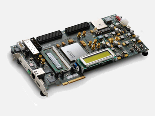
The Virtex™ 7 FPGA VC707 Evaluation Kit is a full-featured, highly-flexible, high-speed serial base platform using the Virtex 7 XC7VX485T-2FFG1761C and includes basic components of hardware, design tools, IP etc.
Overview
This board is currently not available.
Please consider the Virtex 7 FPGA VC709 Connectivity Kit as an alternative.
Product Description
The Virtex™ 7 FPGA VC707 Evaluation Kit is a full-featured, highly-flexible, high-speed serial base platform using the Virtex 7 XC7VX485T-2FFG1761C and includes basic components of hardware, design tools, IP, and pre-verified reference designs for system designs that demand high-performance, serial connectivity and advanced memory interfacing. The included pre-verified reference designs and industry-standard FPGA Mezzanine Connectors (FMC) allow scaling and customization with daughter cards.
Key Features & Benefits
- 40Gb/s Connectivity platform for high-bandwidth and high-performance applications using Virtex 7 VX485T FPGAs
- Hardware, design tools, IP, and pre-verified reference designs
- Supports embedded processing with MicroBlaze, soft 32bit RISC
- Enabling serial connectivity with PCIe Gen2x8, SFP+ and SMA Pairs, UART, IIC
- Advanced memory interface with 1GB DDR3 SODIM Memory up to 800MHz / 1600Mbps
- Develop networking applications with 10-100-1000 Mbps Ethernet (GMII, RGMII and SGMII)
- Expand I/O with the FPGA Mezzanine Card (FMC) interface
Featured AMD Devices
Featuring the ROHS compliant kit including the XC7VX485T-2FFG1761 FPGA
| Logic Cells | 485,760 |
|---|---|
| DSP Slices | 2,800 |
| Memory (Kb) | 37,080 |
| GTX 12.5 GB/s Transceivers | 56 |
| I/O Pins | 700 |

Product Information
Board Features
Featuring the VC707 Evaluation Board

Clocking
- Fixed Oscillator with differential 200MHz output used as the “system” clock for the FPGA
- Programmable Oscillator with 156.250 MHz as the default output and frequency targeted for Ethernet applications but oscillator is programmable for many end uses
- Differential SMA clock input
- Differential SMA GTX reference clock input
- Jitter attenuated clock used to support CPRI/OBSAI applications that perform clock recovery from a user-supplied SFP/SFP+ module
Configuration
- Onboard JTAG configuration circuitry to enable configuration over USB
- JTAG header provided for use with AMD download cables such as the Platform Cable USB II
- 128MB (1024Mb) Linear BPI Flash for PCIe® Configuration
- 16MB (128Mb) Quad SPI Flash
Expansion Connectors
- FMC1 – HPC (8 XCVR, 160 single ended or 80 differential (34 LA pairs, 24 HA pairs, 22 HB pairs) user-defined pins)
- FMC2 – HPC (8 XCVR, 116 single ended or 58 differential (34 LA pairs, 24 HA pairs) user-defined pins)
- Vadj supports 1.8V
- IIC
Communication & Networking
- Gigabit Ethernet GMII, RGMII and SGMII
- SFP+ transceiver connector
- GTX port (TX, RX) with four SMA connectors
- UART To USB Bridge
- PCI Express x8 gen2 Edge Connector (lay out for Gen3)
Memory
- 1GB DDR3 SODIMM 800MHz / 1600Mbps
- 128MB (1024Mb) Linear BPI Flash for PCIe Configuration
- SD Card Slot
- 8Kb IIC EEPROM
Control & I/O
- 5X Push Buttons
- 8X DIP Switches
- Rotary Encoder Switch (3 I/O)
- AMS FAN Header (2 I/O)
Debug & Analog Input
- 8 GPIO Header, 9 pin removable LCD
- Analog Mixed Signal (AMS) Port
Power
- 12V wall adapter or ATX
- Voltage and Current measurement capability
Display
- HDMI Video OUT
- 2 x16 LCD display
- 8X LEDs
What's Inside
VC707 Evaluation Board
Featuring the Virtex 7 XC7VX485T-2FFG1761C FPGA

Full seat Vivado™ Design Suite: Design Edition
Node locked & Device-locked to the Virtex 7 XC7VX485T FPGA, with 1 year of updates

AMS 101 Evaluation Card
Pairs with free AMS Evaluator tool for analyzing analog data, internal temperature and voltage measurements, and saving data to a .csv file

Ethernet Cable

Micro USB Cable

Mini USB Cable

Power Adapter

Power Cord


Resources
Design Tools
| Name | Description | License Type |
|---|---|---|
| Vivado Design Suite Design Edition | The AMD Vivado™ Design Suite is a revolutionary IP and System Centric design environment built from the ground up to accelerate the design for FPGAs and SoCs. | Node locked & Device-locked to the Virtex 7 XC7VX485T FPGA, with 1 year of updates |
Intellectual Property
| Name | Description | License Type |
|---|---|---|
| Memory Interface Generator (MIG) | MIG is a free software tool used to generate memory controllers and interfaces for AMD FPGAs. | No-charge IP |